Door de website toch te gebruiken met deze browser kan de website er anders uitzien dan bedoelt en kunnen wij de veiligheid niet garanderen
Quantum and cryogenic circuits
Quantum technologies, including computing, sensing, communications, information technology, and security, are rapidly emerging thanks to the combination of future challenges in these domains and recent advancements that enable quantum technologies to provide an answer. Solid-state circuits to control and observe a growing number of quantum devices will be essential in successfully realizing such technologies. Since most quantum devices must be operated at deep cryogenic temperatures, circuits must also work at those temperatures to ensure compact, reliable, and, especially, scalable systems. The Einstein Telescope, the next-generation gravitational wave detector currently under development, also requires cryogenic operation and thus cryogenic circuits. MICAS is involved in these efforts and has also invested in the necessary measurement infrastructure.
Research challenges
Better transistor models
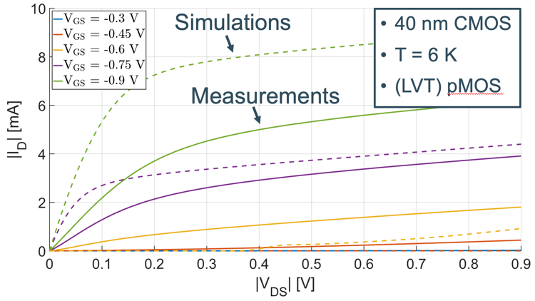
Foundry transistor models are only valid in a limited temperature range, typically between -40 °C – 175 °C. At deep cryogenic temperatures (~4 K), transistors behave significantly differently, and the available models cannot describe this behavior. Currently, the approach is typically to modify the transistor model in a rudimentary fashion, for example, by adjusting the threshold voltage. However, the accuracy of this approach is limited, and it results in circuits that need to be significantly overdesigned. More accurate transistor models are thus required to model the DC transistor characteristics and the noise, matching, and high-speed characteristics. MICAS is currently developing such models based on measured transistors in our cryostat.
Better performance
The lack of transistor models results in circuits performing significantly worse compared to their equivalents at room temperature. For example, recently published cryogenic ADCs have a much worse figure of merit than state-of-the-art ADCs at room temperature. The reason for this is twofold. Firstly, the lack of reliable transistor models leads to overdesign, and thus too high power. Secondly, reliability is often an essential requirement in these applications. For quantum technologies to find their breakthrough, the performance of the circuits needs to increase drastically. Ongoing research at MICAS is addressing this challenge.
Exploiting the cryogenic environment
While the cryogenic environment poses many challenges for the design of circuits, it also provides some opportunities to exploit. The thermal energy at 4 K is ~100x times lower than at room temperature, resulting in almost non-existing thermal noise. This can cause a paradigm shift in the design of many circuits, for example, noise-limited ADCs, analog front ends, etc. Moreover, the carrier mobility increases at deep cryogenic temperatures resulting in many opportunities to design high-speed, high-frequency, or high-power density circuits. These opportunities have not been exploited in the research community. It is an active research direction at MICAS.
F. Tavernier, A. Gatti and C. Barretto, "Chip Design for Future Gravitational Wave Detectors," 2020 IEEE International Electron Devices Meeting (IEDM), 2020, pp. 25.4.1-25.4.4, doi: 10.1109/IEDM13553.2020.9372071.


 Current research topics