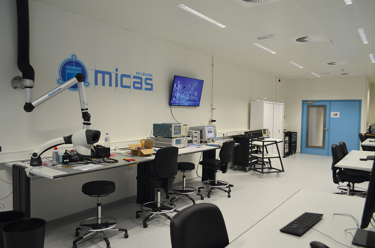
Technology Lab
Chip packaging and modification facilities
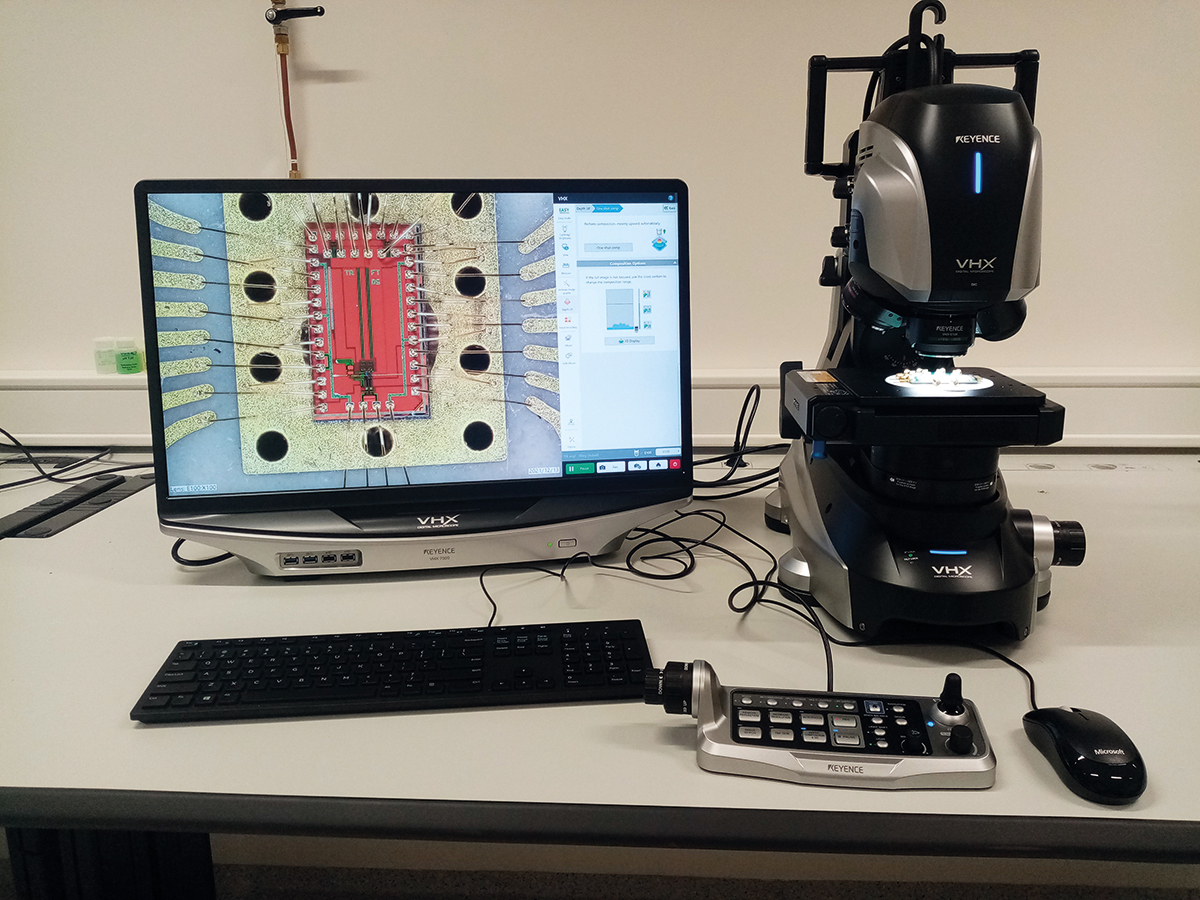
In the MICAS Technology Lab, we have all the necessary chip packaging equipment such as bonding, dicing and flip-chipping tools. For advanced chip modification, a specialized Focused Ion Beam system FIB is available. A 4k-resolution digital microscope can be used for precise imaging, inspection, and three-dimensional measurements on integrated circuits.
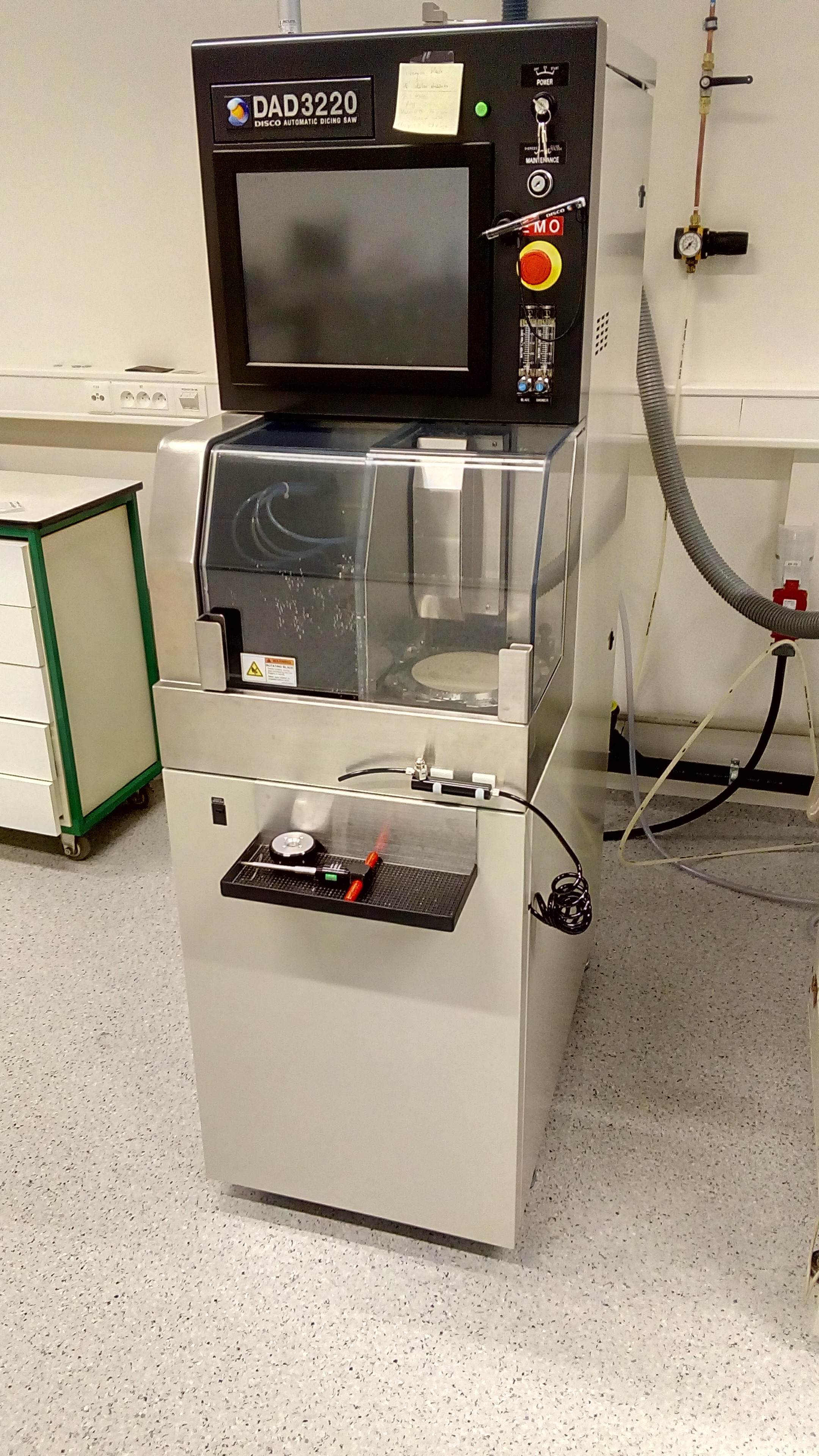
Dicing & grinding
Our Disco DAD3220 dicer can cut silicon wafers up to 160mm in diameter and 0.8mm thickness. Glass wafers can be cut up to a thickness of 2mm. We also cut dies that contain multiple designs into single chips. A specialized CNC controlled grinding machine can perform decapsulation, silicon thinning and polishing of integrated circuits.
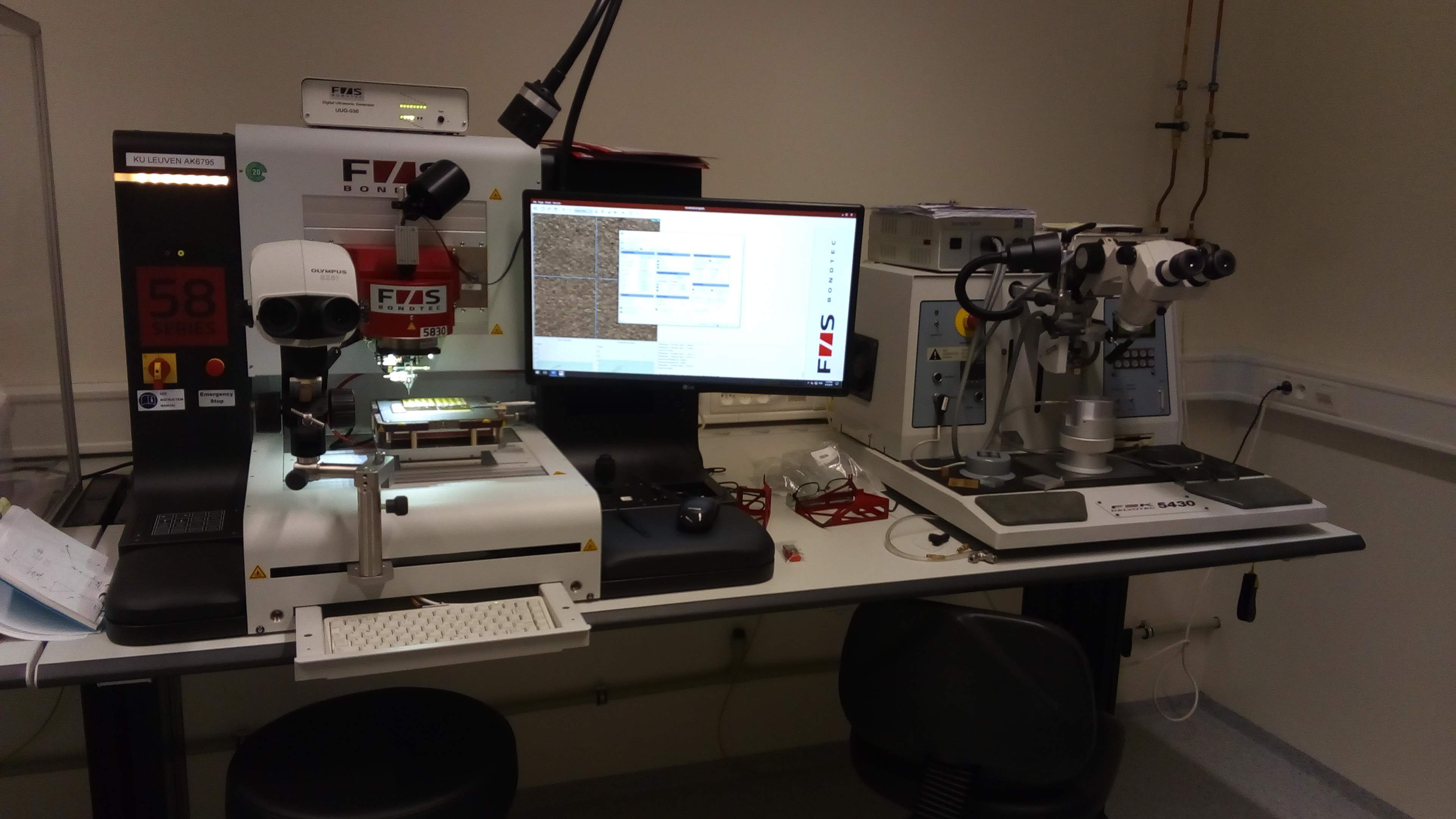
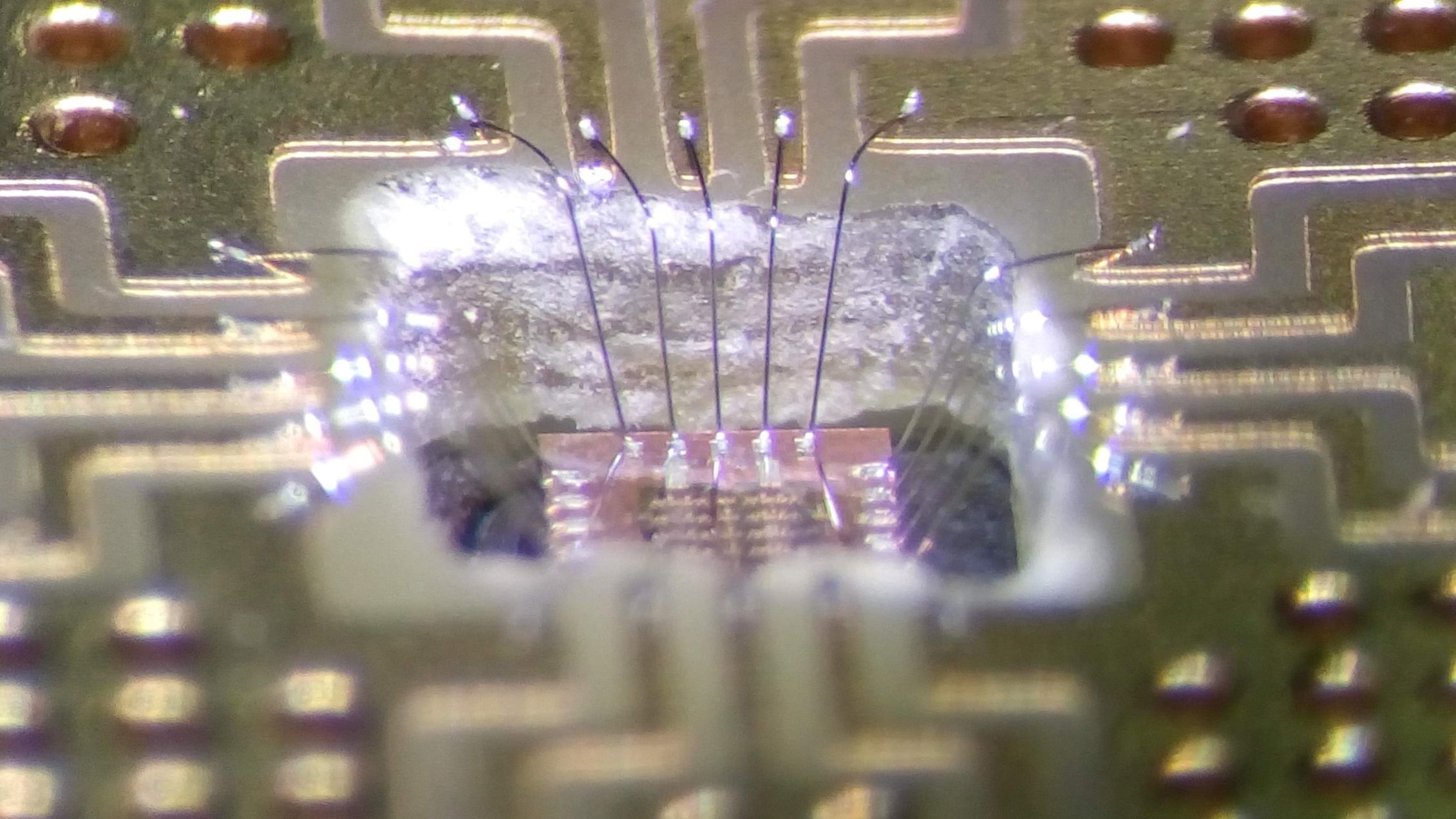
Bonding
The bonding lab is specialized in packaging small series of a wide variety of state-of-the-art chip designs. Wire bonding can be done with both gold and aluminum wires, either on a PCB or in a package.
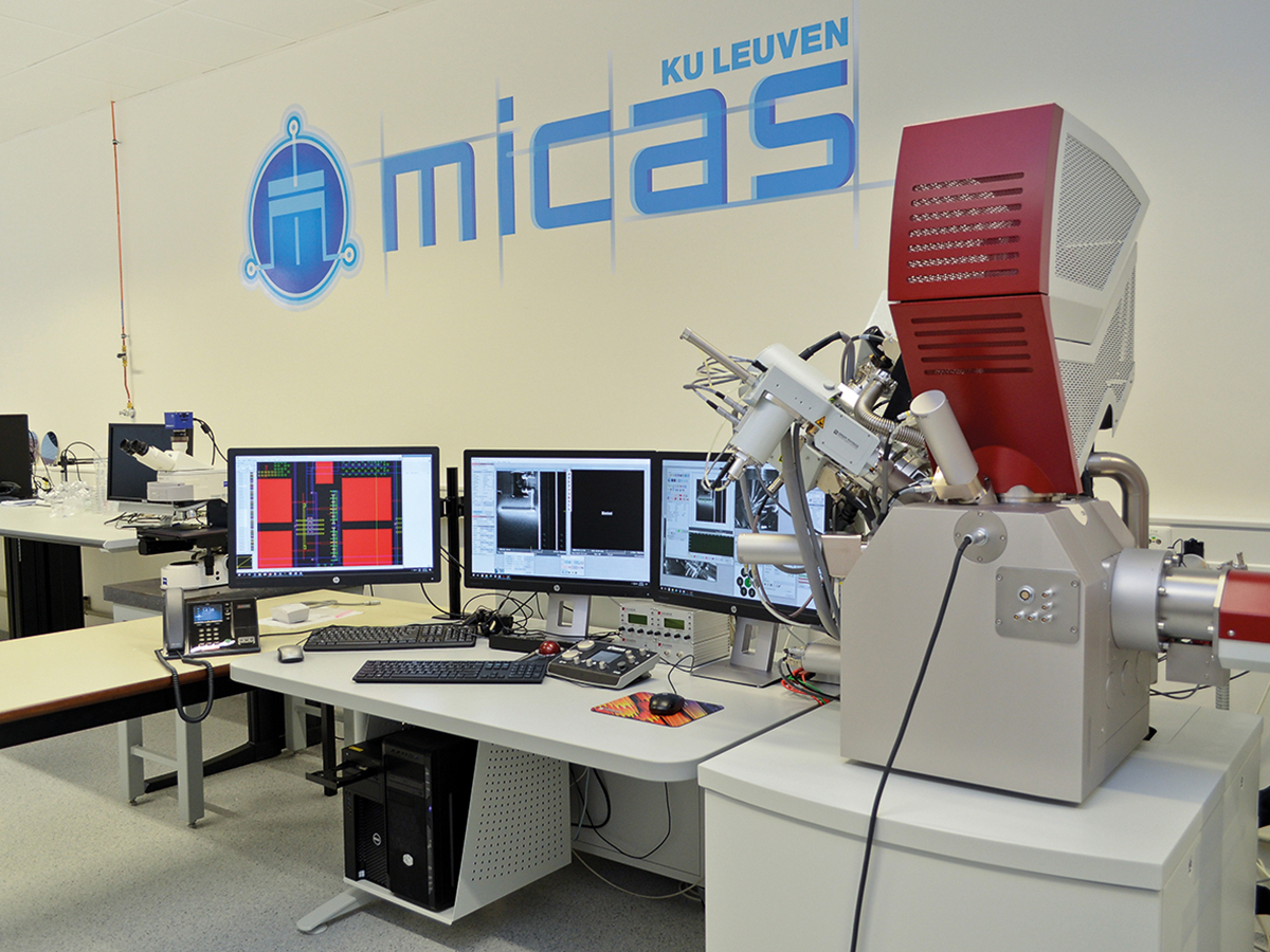
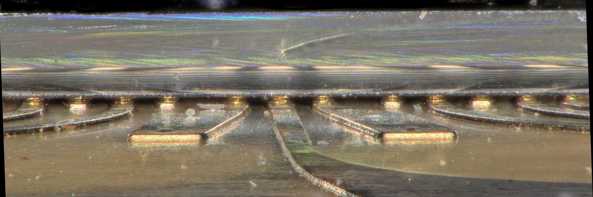
Focused Ion Beam
With our FIB system, several materials can be removed and deposited with nanometer accuracy so that circuits can be modified without the need for re-processing. A unique feature of the system is the increased working distance so that electrical components around the chip do not hinder the repair operation. This allows us to not only make modifications on single dies but even on dies mounted onto a PCB.
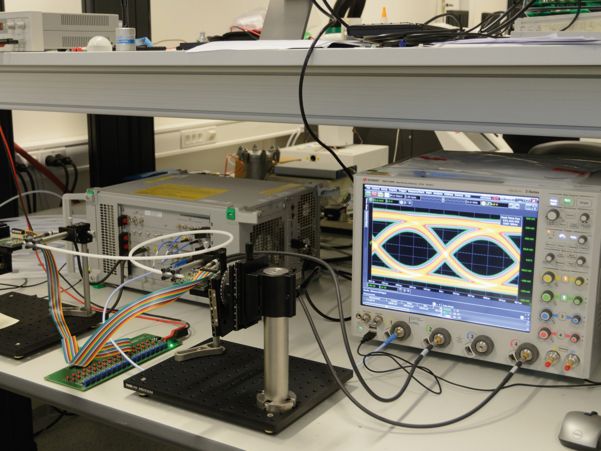
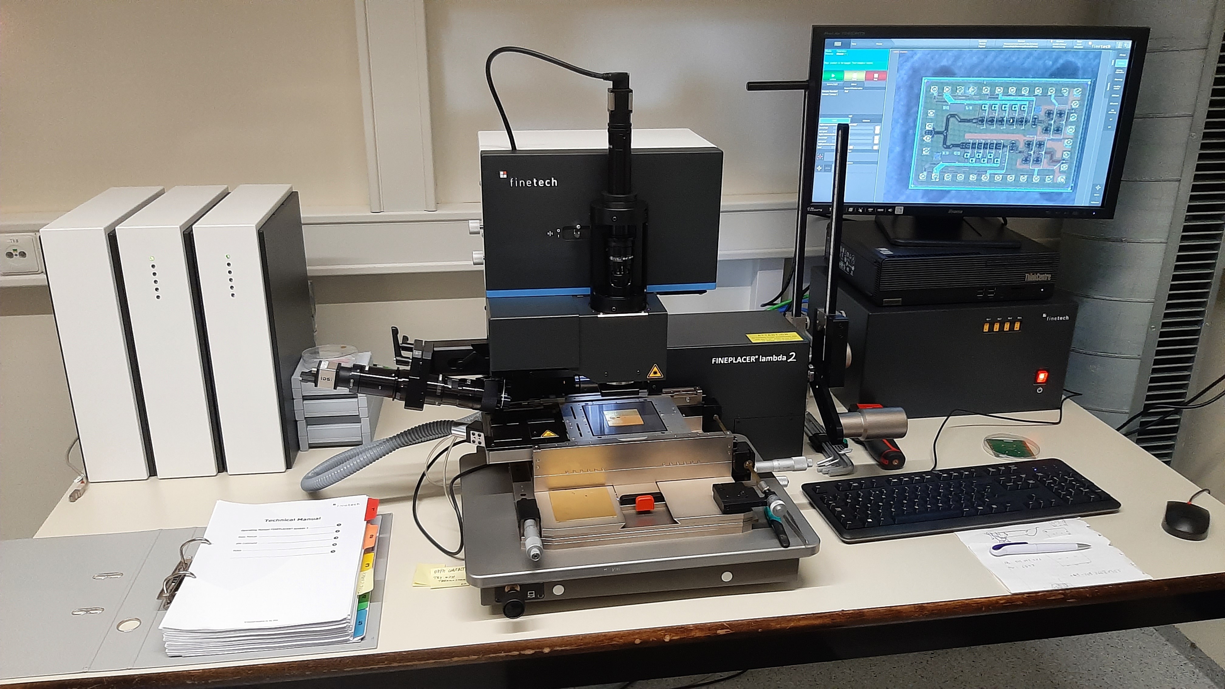
Flip chip
With our Finetech Lambda FINEPLACER machines, we can flip chips with gold studs as well as with copper pillars and solder caps. If needed, we can place the gold studs ourselves with our gold bonding equipment. For chips with up to 40 connections we can use a thermosonic flip chip process at moderate temperatures (~100°C), while for higher amounts of connections we use a thermocompression process at higher pressures and temperatures (up to 300°C).